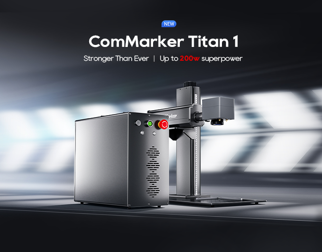
L'importanza dei circuiti stampati (PCB) nell'elettronica moderna
In the world of electronics, Printed Circuit Boards (PCB) serve as the backbone for almost every device, from smartphones and laptops to medical equipment and industrial machinery. These boards provide the physical and electrical connection between various components, enabling them to work together seamlessly. As technology advances and electronic devices become more compact and feature-rich, the importance of PCBs has grown, especially with the need for high-density, affidabile, and efficient circuit designs.
Traditional PCB manufacturing methods, while highly effective, can be complex, time-consuming, and expensive. Enter laser technology – a groundbreaking advancement in PCB production that is transforming the way manufacturers approach circuit design and fabrication. Incisione laser E laser marking technology offer unprecedented precision, velocità, and cost savings, allowing engineers and businesses to meet the growing demands of the electronics industry.
Traditional PCB Manufacturing Methods: Complexity and Limitations
PCB manufacturing has traditionally been a highly involved and complex process. The conventional methods typically include etching, drilling, and milling, which require several steps and various types of machinery. Here’s a brief breakdown of traditional PCB production:
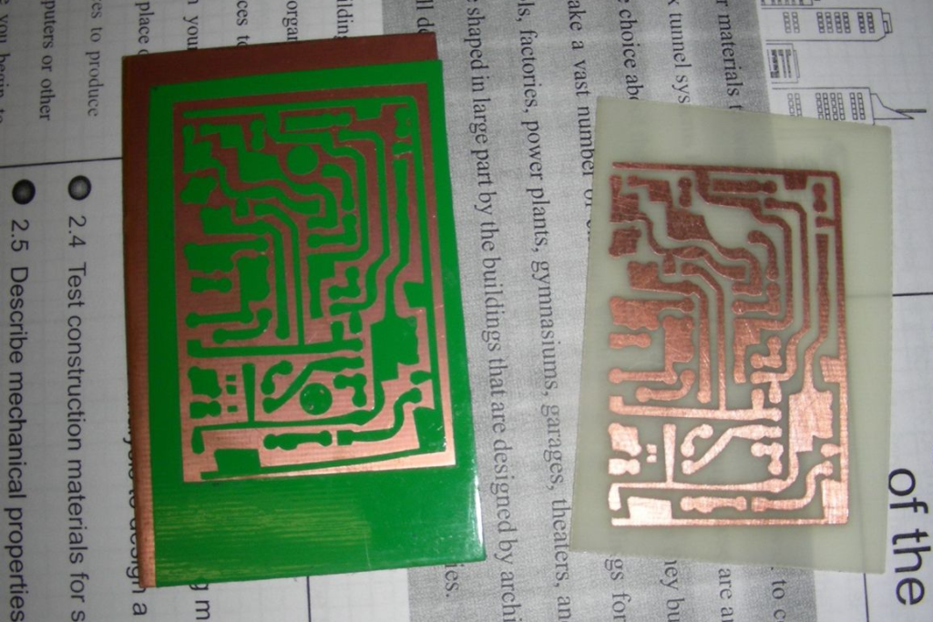
- Etching: The process involves using chemicals to remove unwanted copper from the surface of a copper-clad board, leaving behind the circuit pattern. While this method is effective, it involves toxic chemicals, requires extensive cleaning, and can be time-consuming.
- Drilling: Drilling small holes for vias or electrical connections between layers of the PCB requires high precision and specialized equipment. Traditional drilling methods are slow and may lead to inaccuracies if not carefully controlled.
- Fresatura: In this method, a mechanical tool removes copper from the PCB to form the desired circuit pattern. It’s a precise process but requires time, utensili, e manutenzione.
While effective, these methods come with certain limitations, Compreso:
- Time Consumption: Traditional PCB fabrication can take weeks, especially for prototypes and small batches.
- Complessità: Involves multiple processes, each with its own set of equipment, requiring skilled labor to operate.
- Costo: High overhead costs associated with the equipment, materiali, and labor.
- Inflexibility: Modifications to the design often require new tooling or chemical processes.
This is where laser technology, particularly laser engraving and laser marking, is making a significant impact.
Introduction to Laser Technology in PCB Manufacturing: Precisione ed efficienza
Laser technology in PCB manufacturing is revolutionizing the way circuits are designed and produced. Unlike traditional methods that require mechanical tools or chemicals, lasers use focused light to etch, taglio, or mark materials with unparalleled precision. Laser engraving machines and laser marking systems are now being used in PCB production, offering several key advantages:
- Precisione: Lasers can engrave and etch circuit patterns with micron-level accuracy, making them ideal for high-density circuits.
- Velocità: Laser engraving significantly reduces production time, enabling faster prototyping and small-batch production.
- Efficacia in termini di costi: The elimination of chemical processes and costly tooling means reduced operational costs.
- Flessibilità: Laser systems allow for quick design changes, perfect for rapid prototyping and custom designs.
- Riduzione dei rifiuti: Lasers are highly efficient, minimizing material wastage during the engraving or cutting process.
Ora, let’s explore how laser engraving and laser marking are specifically used in PCB manufacturing.
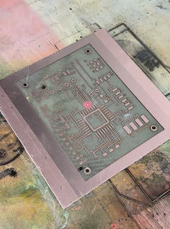
Tecnologia laser nella produzione di PCB
1. Laser Engraving for PCB Prototyping and Small-Batch Production
Laser engraving is an ideal solution for creating high-precision PCBs, particularly when rapid prototyping or low-volume production is required. Here’s how it works in PCB production:
- Fare un passo 1: Circuit Design: PCB designs are typically created using CAD (Progettazione assistita da computer) Software, which outlines the copper traces, vias, and pads required for the circuit. The design file is then fed into the laser system.
- Fare un passo 2: Preparazione del materiale: Copper-clad boards, often made from fiberglass or other composites, are prepared. The copper layer serves as the conductive material for the circuit.
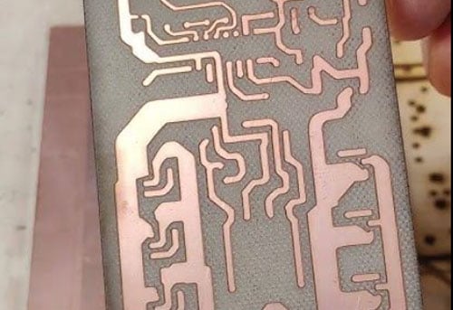
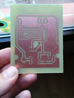
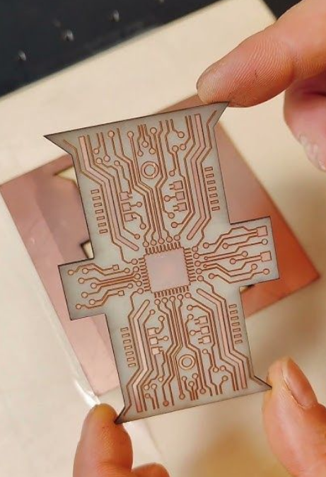
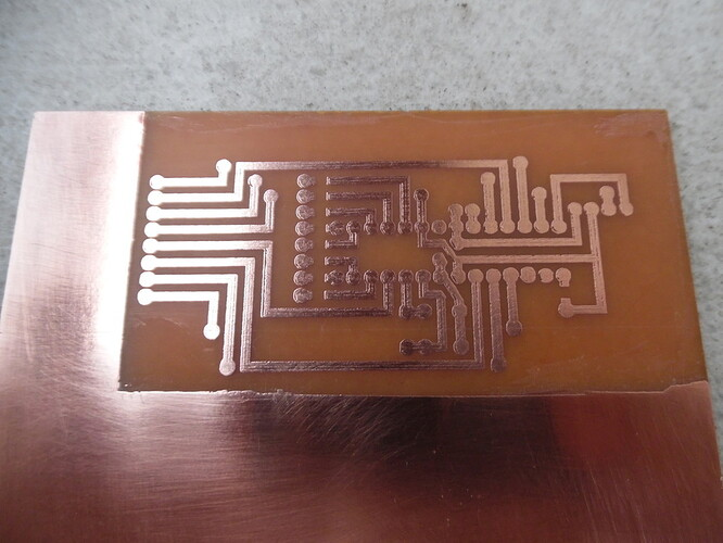
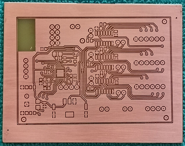
- Fare un passo 3: Incisione laser: Usando il incisore laser, the unwanted copper is precisely etched away along the predefined paths. This high-precision method ensures that the circuit design is accurate to the micron level, even for complex, multi-layered designs.
- Fare un passo 4: Drilling and Cutting: Laser systems can also be used for drilling small vias or cutting the PCB to its final shape. This reduces the need for secondary operations and allows for tighter tolerances.
Laser engraving eliminates the need for expensive masks, prodotti chimici, and complex machinery, making it an ideal choice for small production runs or custom PCB designs.
2. Laser Marking for PCB Steel Stencils
Laser marking plays a crucial role in the creation of PCB steel stencils used for soldering. These stencils help apply solder paste to the PCB during the assembly process. Laser marking machines are used to create these stencils with great precision.
Ecco come funziona:
- Selezione dei materiali: Steel sheets are often used for stencils due to their durability. The laser system marks the steel sheet with the design, leaving precise openings that align with the PCB’s component pads.
- Laser Marking Process: Using a high-power laser, the machine removes a layer of material, creating precise, clean openings without the need for chemical etching or mechanical punching.
- Applicazione: The finished stencils are used in the PCB assembly process, where solder paste is applied through the openings, creating consistent solder joints for components.
Advantages of Laser Technology in PCB Production
Laser technology offers several key advantages when used in PCB manufacturing:
- Alta precisione: Lasers can produce intricate and detailed circuit patterns with micron-level accuracy, essential for modern PCB designs that require high-density circuit layouts.
- Faster Turnaround Times: Laser engraving allows for quicker prototyping and smaller production runs, reducing the time needed to develop new PCB designs. This speed is particularly beneficial for industries that rely on rapid product development cycles.
- Increased Flexibility: Laser systems provide the ability to make design adjustments quickly. A differenza dei metodi tradizionali, where design changes require retooling or new chemical processes, laser systems allow users to modify designs without delay, making them perfect for rapid iteration.
- Reduced Material Waste: Laser engraving is a precise, non-contact process that doesn’t generate waste materials like traditional etching or milling. This precision also means that less material is used, reducing overall production costs.
- Lower Operating Costs: By eliminating the need for chemical processes, specialized tools, and high-maintenance machinery, laser engraving significantly reduces the cost of production, making it more accessible for smaller companies or DIY enthusiasts.
Steps for Laser PCB Manufacturing
Here’s a breakdown of the laser-based PCB manufacturing process:
- Designing the Circuit: Use CAD software to design the layout of the PCB, specifying where the traces, pads, and vias will be placed. The design is converted into a format compatible with the laser engraving machine.
- Preparing the Material: Select the appropriate copper-clad board material and prepare it for engraving. Clean the surface to ensure optimal results.
- Engraving the PCB: The laser engraver etches the copper layer away according to the design file. This process is precise, ensuring that the copper traces remain intact for conductivity.
- Drilling and Cutting: Lasers can also be used to drill vias (for electrical connections between layers) and to cut the PCB into its final shape.
- Surface Treatment: After engraving and cutting, the PCB is cleaned and surface treatments such as coating or protection layers may be applied.
Argomento di studio: Laser Marking of PCB Steel Stencils
To illustrate the versatility of laser technology, let’s consider a case study of using a laser marking system to create a PCB steel stencil.
Materials Used:
- 0.2mm Black PVC film for the stencil.
- Steel for the final stencil sheet.
Processo:
- The laser marking machine creates precise holes in the steel sheet, allowing for accurate solder paste application during the PCB assembly process. The use of a laser ensures that the holes are sharp and clean, reducing defects during the soldering process.
Challenges and Solutions in Laser PCB Manufacturing
While laser technology offers numerous benefits, it is not without its challenges. Here are a few challenges faced during laser PCB production and their solutions:
- Selezione dei materiali: Different materials have different thermal properties, che può influire sul processo di incisione. It’s essential to choose the right material for the PCB to avoid issues such as overheating or incomplete engraving.Soluzione: Use materials that are compatible with the laser’s power settings. Adjust laser parameters to ensure optimal results.
- Laser Parameter Settings: Incorrect power, velocità, or frequency settings can result in uneven engraving or damage to the PCB material.Soluzione: Fine-tune laser parameters based on the material and design to achieve precise, incisioni pulite.
- Precision Issues: Achieving precise and accurate engravings can be difficult if the laser is not properly calibrated or the material is not flat.Soluzione: Regularly calibrate the laser system and ensure that the PCB material is properly secured during the engraving process.
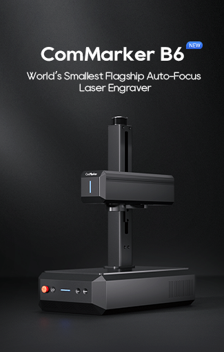
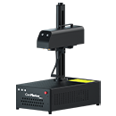
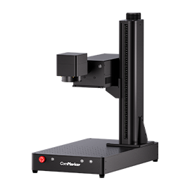
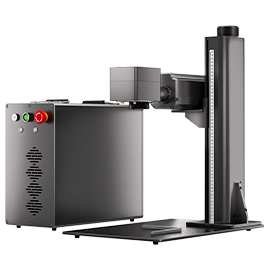
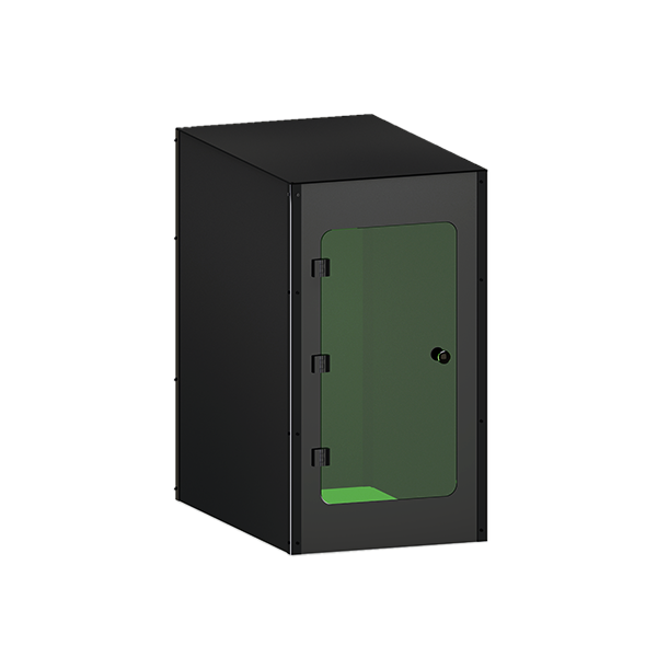
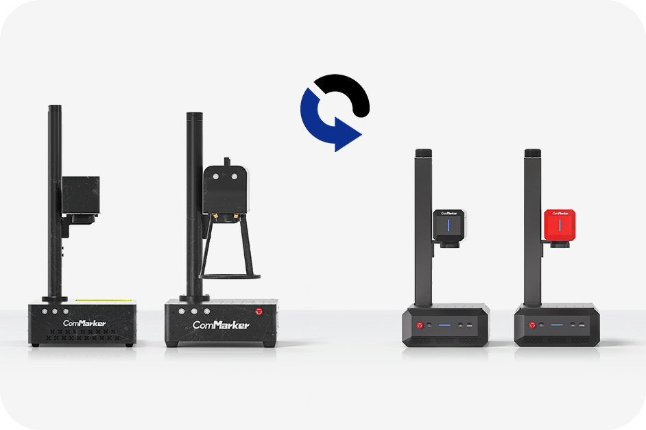
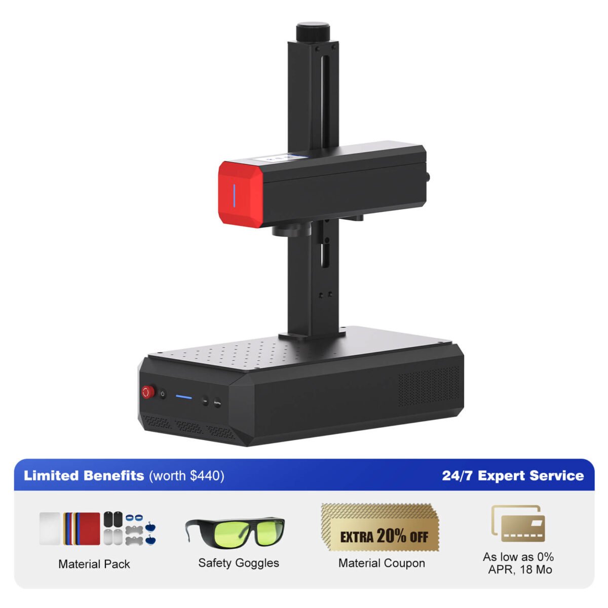
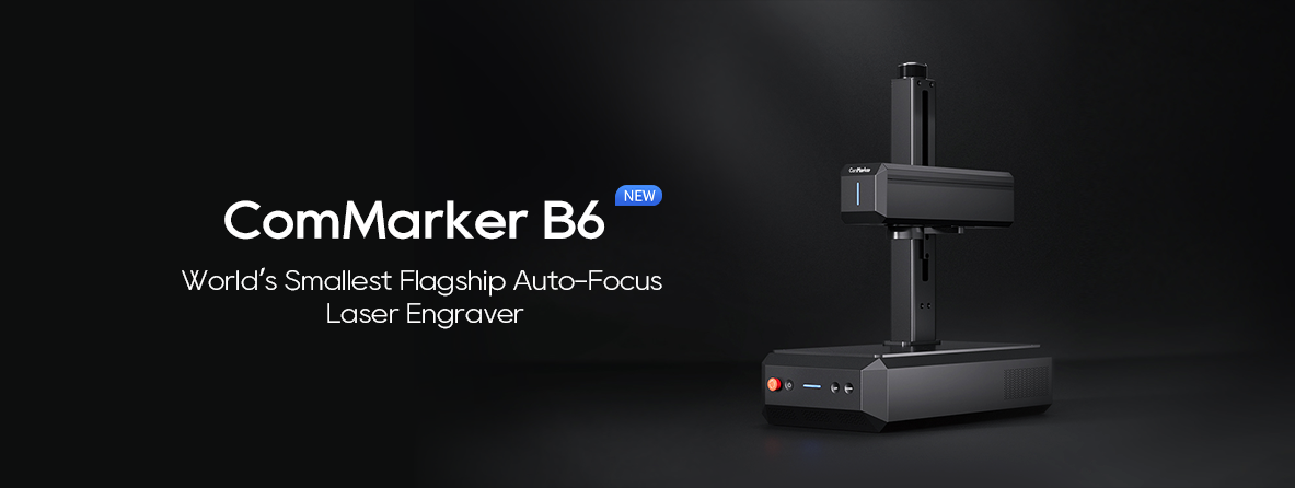
Incisore laser a fibra ComMarker B6 JPT MOPA
Benvenuti nell'era dell'incisione intelligente a colori. Capacità di marcatura del colore di dimensioni compatte da record di record super 3D incisione & Abilità di taglio 2 in 1 Design Tecnologia automatica focus 15.000 mm/s Speedmax ™ Incisione 8K HD Accuratezza Smart LED touch screen
Laser technology is revolutionizing PCB manufacturing by offering high precision, faster turnaround times, and cost-effectiveness. With the ability to engrave and cut a wide variety of materials, compresi i metalli, plastica, legna, e vetro, laser engraving is a versatile solution for both prototype and small-batch PCB production. Whether you’re a hobbyist, engineer, or professional manufacturer, embracing laser technology can help you achieve the precision and efficiency needed to meet the demands of modern electronics.
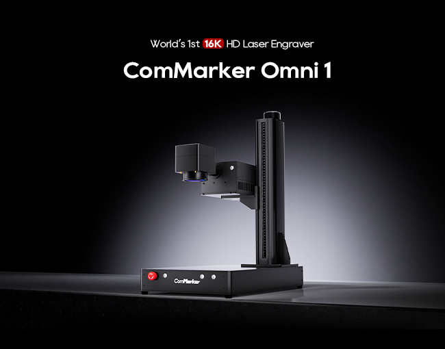
For those looking to explore the potential of laser-based PCB production, ComMarker’s range of laser engravers, including the ComMarker B6 MOPA, offers a powerful and precise solution for PCB production. Whether you’re designing intricate circuit boards for high-density electronics or creating custom designs for prototyping, the ComMarker B6 MOPA Fiber Laser provides the speed, precisione, and flexibility needed to take your PCB manufacturing to the next level.


