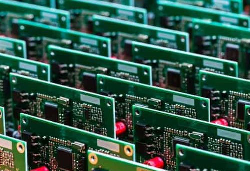


PCB engraving with a fiber laser engraver involves using high-precision laser technology to etch, カット, and mark the various layers and components of a printed circuit board. This method replaces traditional mechanical and chemical processes, providing a cleaner, more accurate, and faster alternative.

Advantages of Using a Fiber Laser Engraver for PCB Engraving
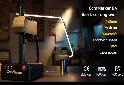
High Precision and Accuracy: Fiber laser Engraver can achieve extremely fine detail, which is crucial for the intricate patterns and connections on a PCB. This precision ensures the reliable performance of the final electronic product.
Efficiency and Speed: Laser cutting is significantly faster than traditional methods, reducing production time. The high-speed galvo technology in fiber lasers swiftly directs the laser beam, allowing for rapid processing.
多用途性: Fiber laser engraver can work with various PCB materials, including FR4, aluminum-based PCBs, and copper-clad laminates. This versatility makes them suitable for a wide range of applications.
Minimal Material Waste: The precision of fiber laser engraving reduces material wastage, which is both economically beneficial and environmentally friendly. It also produces less residue and debris compared to mechanical cutting methods.
Non-Contact Process: Laser engraving is a non-contact process, meaning there is no physical wear on the tool or the PCB material. This results in lower maintenance costs and less risk of damaging delicate components.

Key Features of Fiber Laser Engravers for PCB Engraving
高度なソフトウェア統合: Fiber laser engravers used for PCB engraving often come with software that supports various design formats and allows for precise control over the engraving process. Software like LightBurn and EZCAD2 are commonly used.
High-Speed Galvanometer: This component ensures that the laser beam is accurately directed onto the PCB at high speeds, maintaining precision even with complex designs.
オートフォーカス技術: Advanced fiber laser engravers include auto-focus systems that adjust the laser focus based on the material’s thickness and surface variations, ensuring consistent engraving quality.
Cooling Systems: Efficient cooling systems are crucial for maintaining the optimal performance of the laser engraver, preventing overheating, and ensuring continuous operation.

Applications of PCB Engraving with Fiber Laser Engravers
Prototyping: Fiber laser engravers enable rapid prototyping of PCBs, allowing designers to quickly iterate and test their designs.
Small-Batch Production: For startups and small businesses, fiber laser engravers provide an affordable solution for producing small batches of PCBs without the need for expensive tooling.
カスタマイズ: Custom PCBs for specific applications or projects can be easily produced with fiber laser engraving, offering flexibility in design and functionality.
Repair and Rework: Fiber laser engravers can be used to modify existing PCBs, such as adding new traces or removing damaged sections, facilitating repairs and modifications.

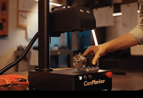
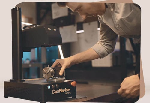
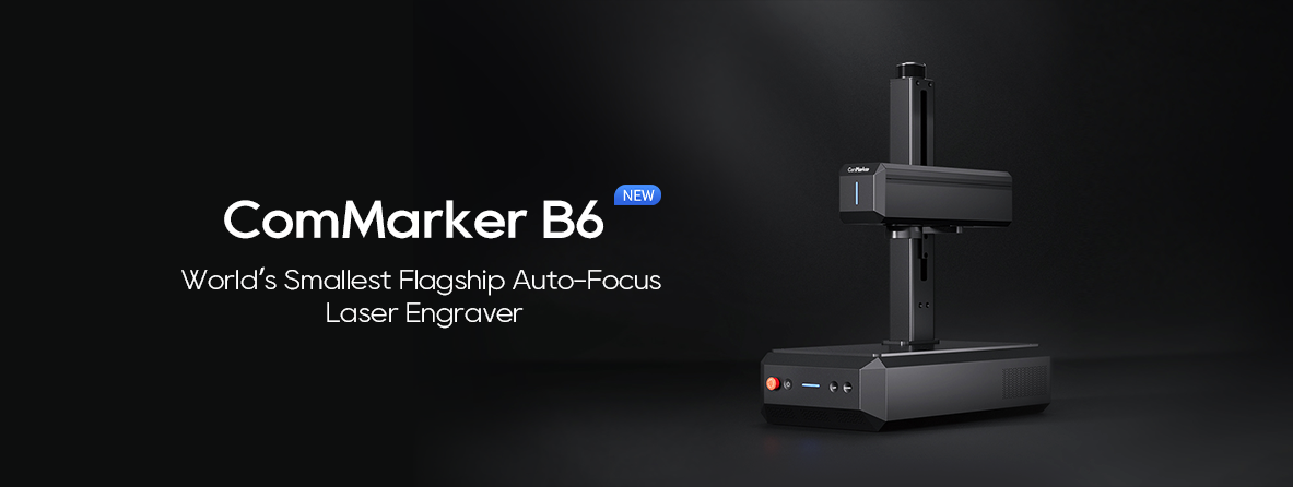
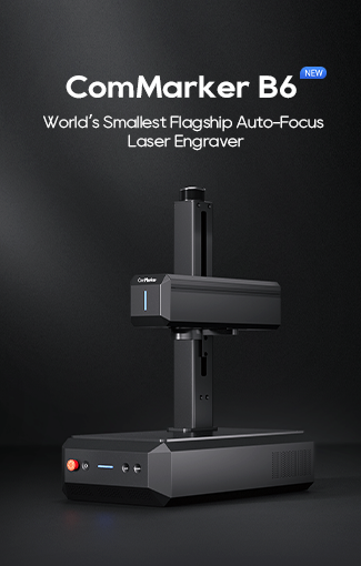
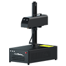
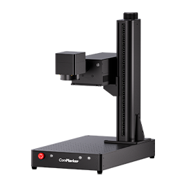
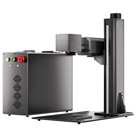
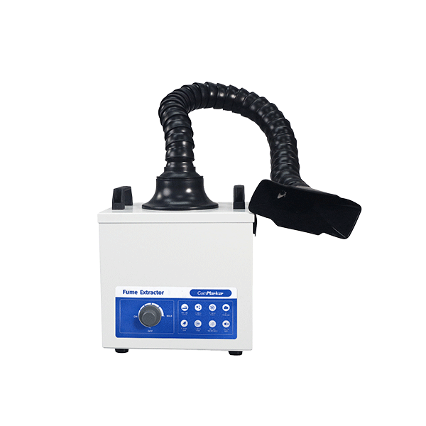
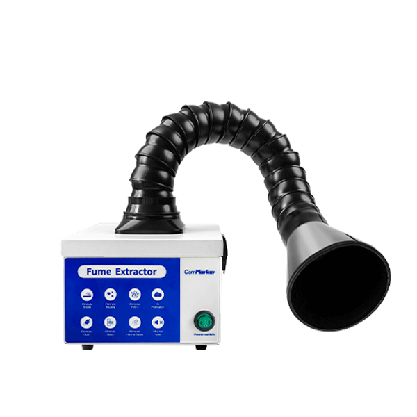
Six-Step Guide to Engraving a PCB with the ComMarker B6 Fiber Laser Engraver
ステップ 1: 回路図を設計する
Begin by meticulously crafting the circuit diagram to match the desired specifications for the PCB board. Accuracy and precision in this design phase are crucial, as they ensure the functionality and reliability of the final product.
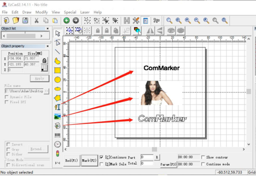
ステップ 2: 回路図をEZCADに入力
Utilize EZCAD’s user-friendly interface to seamlessly transfer your meticulously designed circuit diagram. This software facilitates a smooth transition from the digital design phase to practical implementation on the ComMarker B6 Fiber Laser Engraver.
ステップ 3: パラメータを設定する
Fine-tune the engraving parameters on the ComMarker B6. Consider factors such as power, スピード, と周波数. Proper calibration at this stage is essential to achieve optimal engraving performance and material preservation.
ステップ 4: 位置とサイズをプレビューして調整する
Use the ComMarker B6’s preview functionality to display the circuit diagram on the PCB board. 必要に応じて位置とサイズを調整します, aligning the digital design with the physical dimensions of the PCB board to ensure precise engraving.
ステップ 5: Initiate the Laser Engraving Process
Start the laser engraving process, allowing the ComMarker B6 to etch the digital circuit diagram onto the PCB board. Monitor the procedure closely to ensure it adheres to the set parameters and maintains accuracy throughout.
ステップ 6: 結果を確認する
彫刻後, carefully inspect the PCB board. マーキングが意図した回路設計と一致していることを確認し、彫刻の全体的な品質を評価します。. This final check ensures the accuracy and functionality of the engraved circuit, レーザー彫刻プロセスが成功したことを確認する.